Printed circuit boards (PCBs for short) are firmly established in the world of modern electronics. Because of the enormous possibilities they provide, they are the heart of almost every device, regardless of the industry or application. However, their mass industrial use requires huge production capacities, which resulted in the emergence of highly specialised PCB production plants.
Production of printed circuit boards is a complex technological process
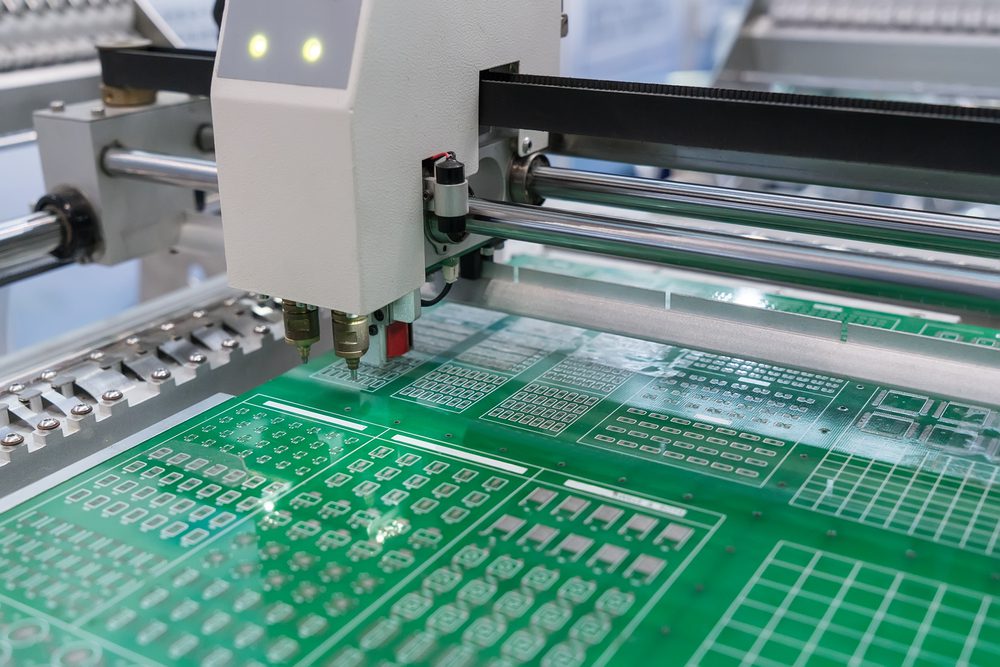
The production of printed circuit boards is now fully automated, which maximises the efficiency of the process itself. Market tycoons are able to produce even several dozen thousand PCBs during a single working day.
Interestingly, these statistics include not only PCB production ordered by regular contractors, but also one-off orders received from individual customers.
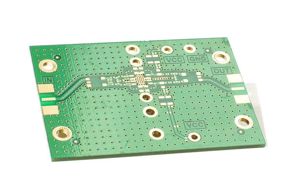
This phenomenon, in a way, is a peculiarity of the market itself – many hobbyists design PCBs on their own, according to the requirements of their project. Additionally, these are often PCB prototypes that undergo minor changes after the first tests. Subsequent iterations land in the factory’s order box, which PCB production must also keep up with.
PCB production step by step
Professional PCB production companies employ engineers with considerable experience in the field of consumer electronics. Their task is to preliminarily verify placed orders – both those from regular wholesale contractors and individual customers placing single orders.
However, this process is largely automated and its primary task is to catch any errors that could lead to a non-functioning PCB. Only after the initial verification is completed, the PCBs are produced.
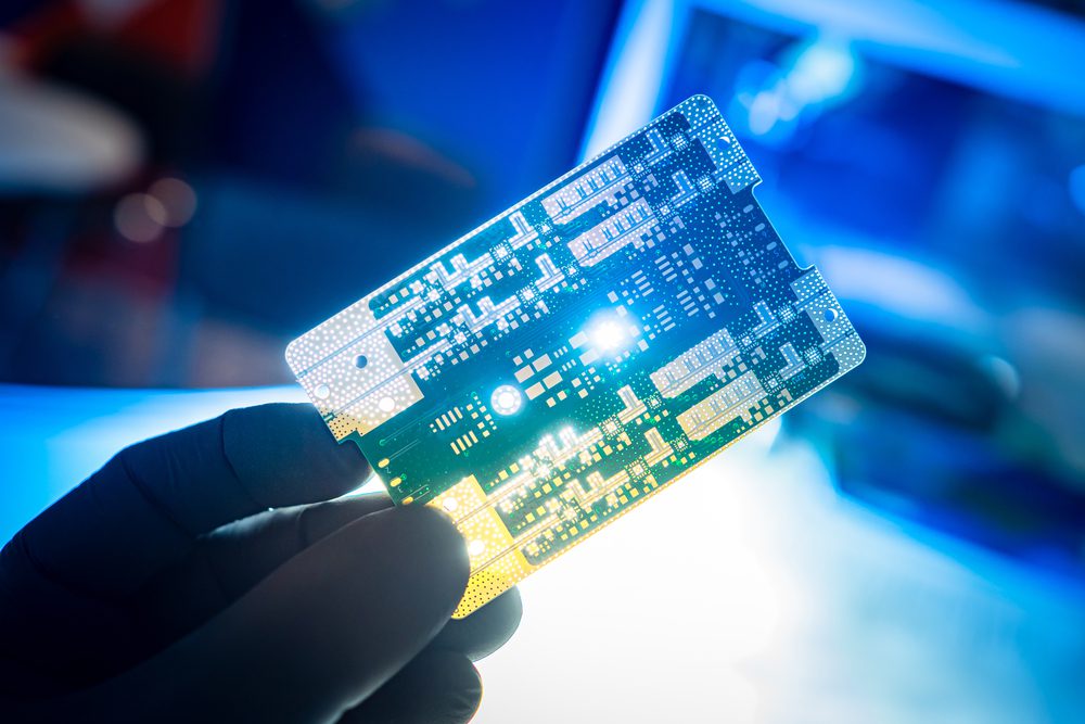
The next stage of work is the preparation of laminate, which will be used to create the PCB. The size and thickness of the PCB are selected for the order, and the material itself is checked for damage or other blemishes.
u00a0
PCB production then moves to the part of the plant where CNC machine tools reign supreme. With their help, the laminate is drilled according to project requirements. This part of the process is also fully computerised – in professional plants, even the changing of drill bits is the responsibility of automation.
Only those parts of the PCB where there are no tracks or other important elements are laminated. After irradiating the PCB with ultraviolet light, the layer hardens, which provides the PCB with high scratch resistance.
Slowly reaching the end, PCB production moves on to the section where the PCB is coated with a thin layer of tin. The excess tin is then removed and the PCB goes to the next section of the factory where the PCB is etched. During this process the tracks, the heart of each PCB, are created.
The final stages of PCB production are the application of soldermask, the coating of unprotected copper fragments and the creation of the description layer. At this point the PCB is also cut in accordance with project requirements.
PCB production ends with PCB testing – automated robots check that all connections have been made correctly. The number of completed PCBs is also verified, and they are then packaged and prepared for dispatch to the end customer.
How useful was this post?
Click on a star to rate it!
Average rating 0 / 5. Vote count: 0
No votes so far! Be the first to rate this post.


