Table of Contents:
Switching power supplies are becoming increasingly common in both consumer and professional electronics. The design of switched-mode power supplies is more elaborate than that of classic linear power supplies, which translates into a slightly more complex process of converting and regulating the output voltage. One of the most popular ICs used in switching power supplies, is the TL494 driver, which we will look at in this article.
TL494 - general characteristics of the circuit
The TL494 IC is a PWM controller dedicated to switching power supplies. The main task of this IC, is to regulate the voltage at the output of the power supply by pulse width modulation (PWM). In this article, we will take a look at the design and functions of this IC and learn about its working principle.
PWM regulation vs. continuous voltage regulation
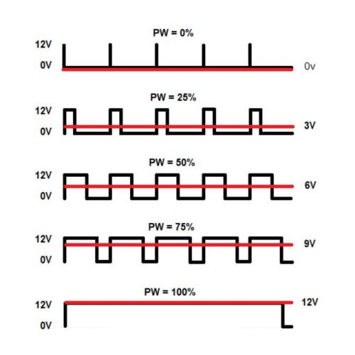
In power supplies based on linear stabilizers (such as ST Microelectronics’ L7812CV ), the voltage regulation process occurs continuously. This is a simple technique that requires a small number of additional components and allows to obtain a stable output voltage free of interference. The disadvantage of such a solution, on the other hand, is very high energy losses. In contrast, the use of regulation through the PWM modulation technique, allows to significantly increase the efficiency of the system. In essence, such a regulation technique consists in rapidly switching on and off the voltage at the output of the power supply by driving the transistors in the power stage in such a way that the voltage obtained at the output of the power supply is, after averaging, equal to the value of the same target DC voltage. The operation of PWM control is described in Figure 1:
According to the presented time waveforms, we can note that the average value of the PWM signal voltage is linearly proportional to the value of the PW fill factor. The fill factor is the duration of the high state (control voltage ON time) in a single cycle of the PWM signal. This means that regardless of the modulation frequency of this signal, its average value is determined by the fill factor. For example, wanting a DC voltage of 6V at the output of the power supply circuit, having a maximum source voltage of 12V, we need to set the fill factor to 50%, but if we needed ideally , “TTL five volts”, then the required fill factor should be 5V/12V = ~41.67%.
TL494 - general characteristics of the circuit
The TL494 IC is a PWM controller specifically designed for power supply circuits operating on the pulse width modulation principle. The TL494 IC contains built-in all the necessary functional blocks for realizing a pulse power supply circuit. Its components include a built-in control signal generator with frequency adjustable by changing the values of the externally attached R and C elements that make up the timing circuit, a dead-time regulator (DTC) stage, two voltage comparators with two error amplifiers, a pulse-triggered flip-flop that controls the output transistors, and a precision 5V stabilized voltage source.
TL494 - circuit pinout description
The following is a description of the individual pinouts of the TLT494 IC, housed in a DIP16 enclosure for through-hole mounting (THT):
1 – 1 IN+ – non-inverting input of error amplifier #1
2 – 1 IN- -inverting input of error amplifier #1
3 – FEEDBACK – feedback signal from output to input of the system
4 – DTC – input of the internal amplifier that controls the dead time of the system
5 – CT – capacitor of the external timing circuit
6 – RT – resistor of the external timing circuit
7 – GND – system ground
8 – collector of output transistor Q1
9 – emitter of output transistor Q1
10 – emitter of output transistor Q2
11 – collector of output transistor Q2
12 – VCC – positive supply voltage rail
13 – O/P CNTRL – pin for configuring the way the circuit output works (push-pull or single-ended)
14 – REF – output of built-in +5V reference voltage source
15 – 2 IN- -inverting input of error amplifier #2
16 – 2 IN+ – non-inverting input of error amplifier #2
TL494 - permissible maximum values of operating parameters of the system
The TL494 circuit can be supplied with a maximum voltage of 41VDC. The allowable voltages applied to the measurement inputs of the comparators must be between -0.3V and the supply voltage minus 2V. The maximum output voltage on the collector of the internal transistor is 41V, and the maximum collector current up to 250mA per channel. The soldering time of a single pin must not exceed 10s at 260*C.
TL494 - recommended operating conditions
In order for the TL494 IC to work properly, certain conditions must be adhered to. The circuit’s supply voltage range is between 7V and 40V, and the input voltage range of the error amplifier is between -0.3V and the VCC value minus 2V (e.g., 13V for a 15V VCC supply). For transistors in the output stage, the collector-emitter voltage can be no more than 40V and the collector current 200mA. The current supplied to the FEEDBACK input can be a maximum of 0.3mA. The frequency range of the built-in control signal generator is between 1kHz and 300kHz. The recommended values of the R and C elements of the external timing circuit are 1.8k to 500k for the resistor and 470pF to 10uF for the capacitor, respectively.
The dead-time control circuit’s comparator is set to a fixed offset value to ensure a constant dead time of approximately 5%. The function of the built-in timing generator can be bypassed by connecting the chip’s RT pin No. 14 to the REF reference pin and externally supplying a sawtooth signal to CT pin No. 5. This function also allows synchronous control of multiple TL494 chips having different power rails. The output transistors inside the chip having floating outputs are arranged to provide an output with a common emitter or an output with an emitter secondary. The chip allows the user to achieve a push-pull or single-ended output stage on the output pins by properly configuring pin 13, which is the output control function pin. Internal circuitry prevents any of the outputs from generating a double pulse when the IC has the output configuration as push-pull.
How useful was this post?
Click on a star to rate it!
Average rating 4.5 / 5. Vote count: 4
No votes so far! Be the first to rate this post.

