Table of Contents:
The world around us is an analog world, i.e. one in which the physical quantities describing it change continuously and can take any value from the set of real numbers. In contrast, when it comes to computers or electronic measuring devices, digital technology dominates. In order, for example, for a measuring instrument such as an electronic scale to be able to understand what the value of the quantity it is measuring is and to display information about it on its display, what is needed here is a complex design of the measuring system, in which one of the key elements is an analog-to-digital converter, such as, for example, the HX711 discussed in the current article.
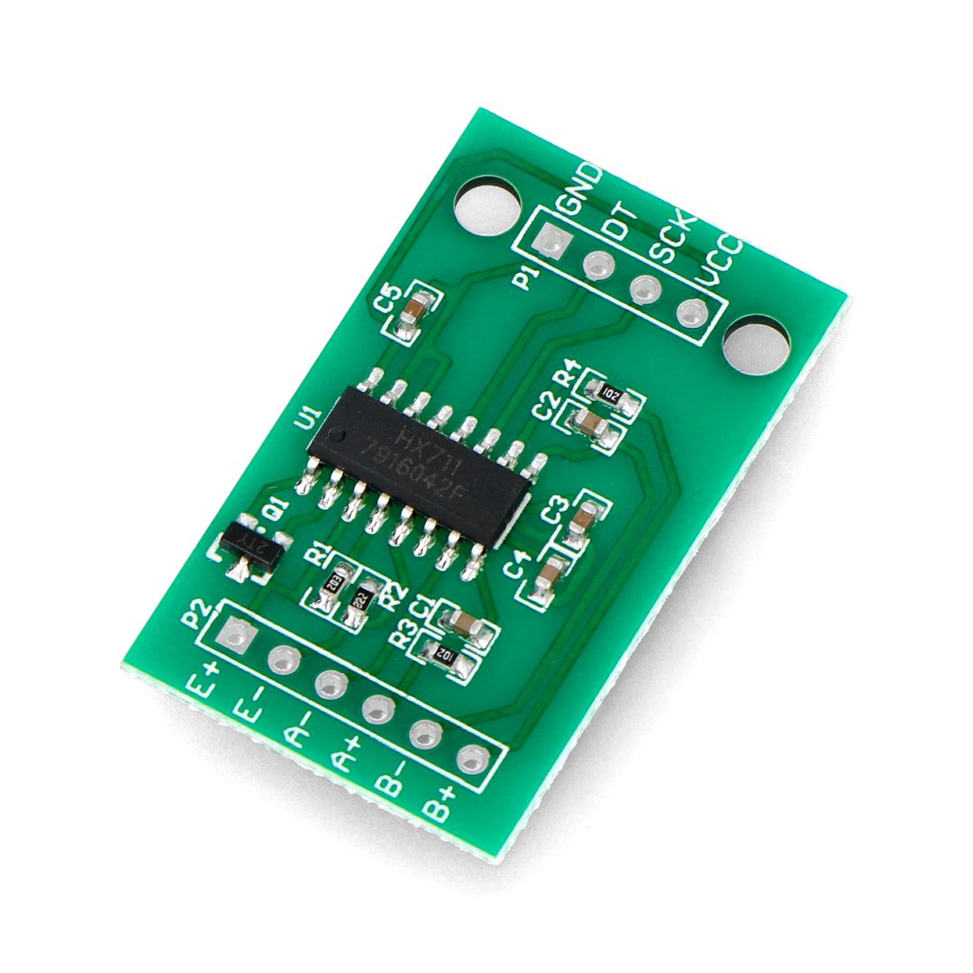
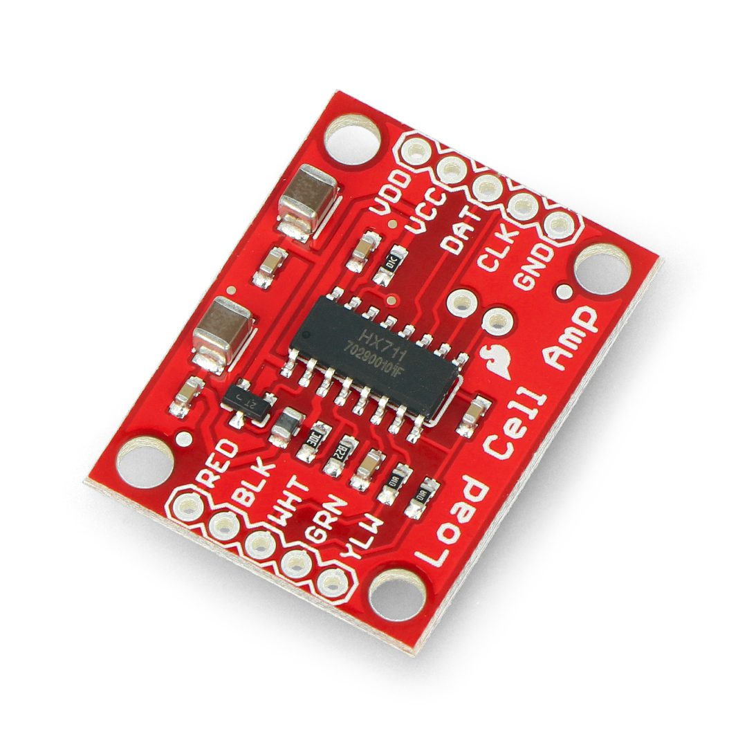
HX711 - general characteristics of the system
The HX711 from Avia Semiconductor, is a precision 24-bit analog-to-digital converter designed for electronic measurement applications with the highest accuracy for professional purposes. The key features of this chip are:
- Two selectable channels with differential inputs,
- Built-in low-noise programmable input gain with the option to select the gain factor among values of 32, 64 and 128,
- built-in voltage stabilizer for analog and digital part
- built-in clock signal generator eliminating the need to connect an external quartz resonator,
- A built-in reset circuit that is triggered every time the power is turned on,
- simple communication interface, simple digital control and serial interface,
- No need to program the system,
- Selectable output data rate between 10SPS and 80SPS,
- Built-in filtering circuit for 50Hz and 60Hz mains voltage frequency,
- low current consumption during operation and at rest – less than 1.5mA and less than 1uA, respectively,
- Power supply voltage range from 2.6V to 5.5V,
- operating temperature range from -40*C to +85*C
- 16 pin surface mount housing
HX711 - description of the leads
1 – VSUP – voltage of the built-in stabilizer: 2.7V – 5.5V
2 – BASE – output controlling the supply voltage of the analog part (not connected when not in use)
3 – AVDD – supply voltage of the analog part: 2.6V – 5.5V
4 – VFB – control voltage of analog part (short circuit to AGND when not connected)
5 – AGND – ground of the analog part
6 – VBG – reference voltage of analog part, bypass type output
7 – INA- – inverting analog input of channel A
8 – INA+ – non-inverting analog input of channel A
9 – INB- – inverting analog input of channel B
10 – INB+ – analog non-inverting input of channel B
11 – PD_SCK – digital disable input (active in high state) and clock input
12 – DOUT – digital serial data output
13 – XO – digital input/output for quartz resonator (not connected when not in use)
14 – XI – digital input/output for quartz resonator (not active for active built-in clock source)
15 – RATE – digital control signal input/output, in low state: 10Hz; in high state: 80Hz
16 – DVDD – Digital part supply voltage: 2,6 – 5,5V
Power options for the HX711 chip
The supply voltage of the HX711 IC for its digital part must be the same as the supply voltage of the microcontroller that works with it. To ensure correct operation, when the internal supply voltage stabilizer for the analog part is used, the dropout voltage of this regulator depends on the characteristics of the external transistor. The output voltage is equal to VDD = (VBG*(R1+R2))/R1 – this voltage value should be a minimum of 100mV less than the value of the supply voltage applied externally to the circuit. If the built-in supply voltage stabilizer of the analog part is not used, the VSUP pin should be connected to the AVD or DVDD pin, whichever voltage is higher. The VFB pin should be connected to ground and the BASE pin should not be connected – then it is not necessary to use the connection of an external 100nF capacitor, normally connected between the VGB pin and ground.
Clock source
By shorting the X1 pin to ground, the clocking source is the internal signal generator. The rated output data rate in this situation is 10 (RATE pin in low state) or 80SPS (RATE pin in high state). If a more precise data rate is required, then an external clocking source in the form of a quartz resonator or other precise clock source should be used. The quartz resonator can then be connected in parallel between pins X1 and X0 via a 20pF coupling capacitor. It is not required that the external clock give a perfectly rectangular waveform – the clocking signal can also be taken from the output of the microprocessor, provided that its amplitude does not exceed 150mV. Using an external clocking signal source, deactivates the built-in oscillator.
Output data format
When using an on-chip oscillator, the output data rate is typically 10 (RATE pin in low state) or 80SPS (RATE pin in high state). When using an external clock or quartz resonator, the output data rate is directly proportional to the clock frequency or quartz frequency. Using an 11.0592 MHz clock or quartz crystal, it gives accurate results of 10 (pin RATE in the low state) or 80SPS (pin RATE in the high state). The output 24 bits of data are completed to a complete binary format. When the input differential signal in the 24-bit range disappears, the output data will be reached at the minimum or maximum value, viz. 800000h (MIN) or 7FFFFFh (MAX), until the input signal returns to the input range.
Serial interface
The PD_SCK and DOUT pins are used for data transmission, data download, input selection, gain selection and shutdown. When the output data is not ready for download, the DOUT digital output pin is in the high state. The serial clock of the PD_SCK input should be in the low state. When the DOUT output goes low, it will indicate that the data is ready for download. By applying 25 ~ 27 positive clock pulses to the PD_SCK pin, data is shifted from the DOUT pin. Each PD_SCK pulse shifts by one bit, starting with the MSB bit, until all 24 bits are shifted. The 25th pulse on the PD_SCK input will flip the DOUT pin back to high. Input selection and gain is controlled by the number of PD_SCK input pulses. PD_SCK clock pulses should not be less than 25 and more than 27 in one conversion period to avoid the occurrence of serial transmission errors.
How useful was this post?
Click on a star to rate it!
Average rating 0 / 5. Vote count: 0
No votes so far! Be the first to rate this post.