Table of Contents:
A phototransistor is an electronic component that combines the functions of a transistor and a photodiode. What is its mechanism of action and what can it be used for?
What is a phototransistor?
Phototransistor is one of the variants of the transistor, which is an electronic component consisting of three layers of semiconductor with varying types of conductivity: emitter, base and collector. Standard trans istors are current-controlled, while in the case of phototransistors the change in value on the collector is dependent on the intensity of light. Therefore, it can be said that components of this type combine the properties of a photodiode and a transistor, and the basis. The basis of their application is the dependence of the value of the larger current between the base-collector junction on changes in the value of the smaller current flowing in the base-emitter junction.
A distinctive feature of phototransistors is that they are much more sensitive to light than standard components of this type, which can be achieved by exposing the base terminal. As a result, it is possible to precisely change the current flowing between the emitter and collector in response to changes in illumination. This makes phototransistors applicable, among others. In various types of optical sensors.
How does a phototransistor work?
Work phototransistor is based on the use of the basic concept of operation of a bipolar transistor. These types of components can be created by exposing the semiconductor of an ordinary transistor to light – mostly they are of almost identical design, differing only in the absence of a housing at the base terminal. As a result, electrons released by light incident on the semiconductor can cause the base current to flow, which is proportionally transferred to the collector.
In phototransistors, the value of the current at the base-collector junction is controlled by the intensity of light incident on the semiconductor. Photons polarize the junction in the direction of conduction, so that a current begins to flow at the output with a value that depends on the value of the illumination. When the transistor is not illuminated, it does not conduct current.
What are the differences between a phototransistor and a standard transistor?
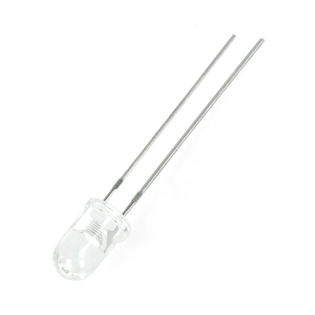
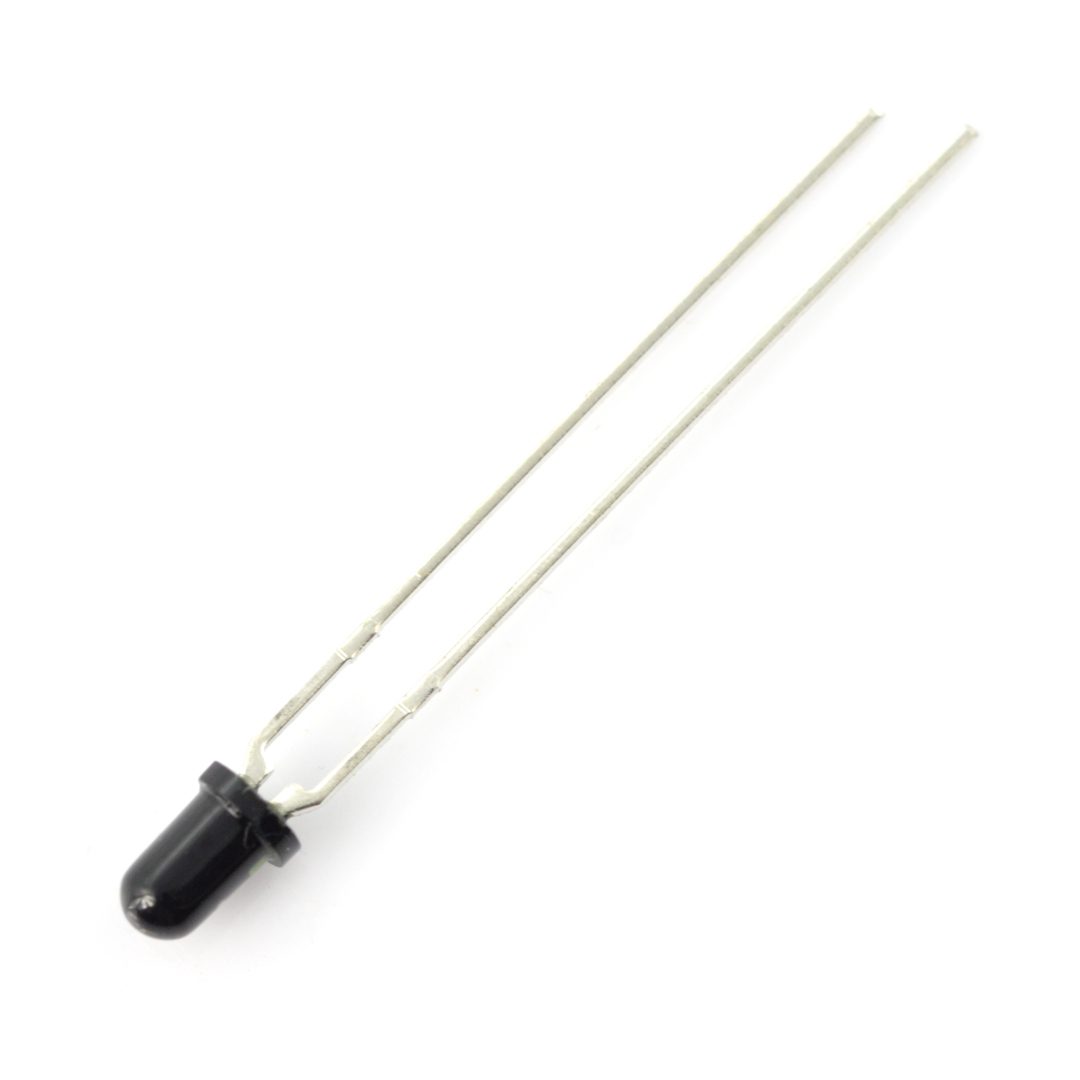
The construction of a phototransistor is very similar to an ordinary transistor. However, the differences may be in the semiconductors used, as well as in the housing of the component. With standard variants, primarily germanium and silicon are used – although they can also be used in phototransistors, a more common sight these days, among others. Gallium, which features a much stronger light response. The housing, in turn, is constructed to allow light to fall on the base area: transparent plastic, for example, can be used for this purpose. What’s more, phototransistors usually do not use an outward leading of the base.
Photodiode vs. phototransistor
Both the photodiode and phototransistor convert light energy into electrical energy. However, these are components with slightly different applications, due to differences in their properties. In particular, the following points should be noted:
- The current gain of the phototransistor is greater than that of the photodiode (when the same amount of light falls on both elements);
- A phototransistor has a higher sensitivity than a photodiode;
- A photodiode can be transformed into a phototransistor;
- A phototransistor may be more compact and easier to use than a photodiode along with additional amplification circuits, if those are in use;
- Phototransistors are often less sensitive to temperature changes than some photodiodes – this is especially important in situations where thermal stability is important.
Phototransistor - application
One of the most important features of phototransistors is their high sensitivity, which is combined with a rapid change in the output value in response to changes in the intensity of light incident on the base. For this reason, they are often used in highly dynamic systems designed for radiation detection. We are mainly talking about measurement systems, such as analog-to-digital converters. However, this is just one of many possible areas of use for phototransistors – components from this family are also used, among others. In security systems, counting systems or systems used to control lighting.
In addition, phototransistors can be found in many everyday appliances whose functionality is based on responding to light. Among the devices that use such elements are CD players and smoke detectors, for example. In addition, phototransistors are used in infrared receivers and in systems that use lasers to detect light.
What are the advantages and disadvantages of phototransistors? How to select a phototransistor for a specific application?
Among the advantages of phototransistors is the fact that they are high-gain devices with relatively high sensitivity. They are also among the relatively inexpensive components, allowing them to be used seamlessly in many projects. Also noteworthy is the ability to easily connect to the chip of your choice via standard leads.
However, phototransistors will not always be the optimal choice – remember that components of this type cannot handle the high voltages of other semiconductor devices, such as phototristors. They are also susceptible to mechanical damage that exposes them, among other things. For transient voltage spikes or surges.
To select a phototransistor for a given project, it is useful to suggest the current-voltage characteristics of the product and determine the correct operating point of this element. The key issue is usually the wavelength for which the phototransistor achieves the highest sensitivity.
Where to look for high-quality phototransistors?
Phototransistors are part of the rich assortment of the store Botland. We offer phototransistors with a variety of characteristics – with maximum sensitivity for wavelengths of 570 nm, 870 nm, 925 nm or 940 nm. It is worth noting that they can be used for both visible light and infrared radiation work. Take a look at our assortment – with us you will prepare projects of almost any functionality!
How useful was this post?
Click on a star to rate it!
Average rating 4.5 / 5. Vote count: 2
No votes so far! Be the first to rate this post.