



New arrivals


On Sale



Fototranzystory - Elementy optoelektroniczne
Semiconductor elements have played a huge role in shaping modern electronic systems. First bipolar transistor was invented in the first half of the 20th century. The bipolar transistor is made of three semiconductor layers with different types of conductivity (p-n-p or n-p-n), which results in two types of bipolar transistors - PNP and NPN. The individual layers have their names: E - emitter, B - base, C - collector. The basis of the use of the transistor is the dependence of the value of the greater current flowing between the emitter-collector junction, on the changes in the value of the lower current flowing in the base-emitter junction.
Products
See also
Phototransistors
Phototransistor in theory
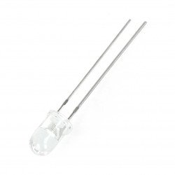
Using the photoelectric properties of semiconductors, a modified version of transistors was invented - phototransistors. In phototransistors, the value of the current in the emitter-collector junction is controlled not by the base-emitter current, but by the intensity of light falling on this junction. Photons falling on the base-emitter junction polarize it in the forward direction, thus causing a current to flow in the emitter-collector junction, the value of which depends on the illumination intensity. In the off-light state, the transistor does not conduct current through the emitter-collector junction, which is equivalent to the off state. Due to the fact that there is no need to supply the base-emitter junction with electricity, phototransistors usually have only two terminals - the emitter and the collector. There are also phototransistors available where the base is connected and can be controlled like a regular bipolar transistor. The advantage of phototransistors over other photoelectric elements, such as photoresistors, is a much shorter switching/response time and much greater sensitivity.
Phototransistor parameters
If you want to correctly select phototransistors for your applications, use the manufacturer's current-voltage characteristics to determine the operating point of the phototransistor appropriate to your needs. An important parameter is the wavelength at which the phototransistor achieves maximum sensitivity. At Botland you will find phototransistors with maximum sensitivities for wavelengths of 570 nm, 870 nm, 925 nm, 940 nm, which covers visible and infrared radiation.
Application
Due to their very high sensitivity and speed of operation, phototransistors are used in radiation detection, where high dynamics of the system is required, therefore in high-speed measurement systems, as analog-to-digital converters, the systems are connected optoelectronically. You can use them as an optocoupler to exchange signals between two electronic systems. Check out the Botland offer and discover the possibilities of phototransistors!
Phototransistors - FAQ
A phototransistor is an optoelectronic element - the current value at the emitter-collector junction is controlled by the intensity of light that falls on the junction. These types of elements are used, for example, as optoisolators, thanks to which the signal is transmitted via light.
A phototransistor is a transistor that responds to changes in light intensity, which results in changes in current at the emitter-collector junction. In an ordinary transistor, such changes are influenced by the current at the base-emitter junction. In a phototransistor, photons that land on the base-emitter junction polarize it in the forward direction, thus allowing current to flow through the emitter-collector junction.
Optoelectronics are electronic components that use light - for example, they actively respond to light or can emit it themselves. Optoelectronic elements include, for example, displays and LEDs, photoresistors , phototransistors and photodiodes.