


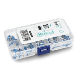


Designing a new device often requires very advanced work. Experienced designers perfectly understand the phenomenon of prototypes, i.e. a prototype of a device for the right one. This is what we start every project with. We can decide to design a new device, but you have to be aware of the difficult, hard and advanced work. For some people, high costs are also an obstacle, which are associated with it. The alternative is a universal PCB, with which we can check and test the electronics. Universal boards differ in construction and size. Its choice must not be accidental, but should depend on the electronic elements used in this particular circuit. We will choose another board for a simple circuit, and another for a more complicated one. In our offer there are many types of universal boards, which we recommend for prototyping for beginner electronics and robotics, as well as for the more experienced ones.

- Sale
- Sale
- Reduced price
- Sale

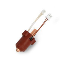
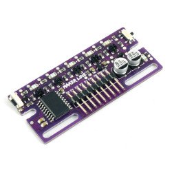
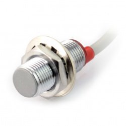
Electrical Actuator Super Power Jack 2000N 7,5mm/s 12V - 44cm stroke
Index: MOT-05365
- Reduced price
- Sale
- Reduced price
- Sale

Circuit boards
Loading...
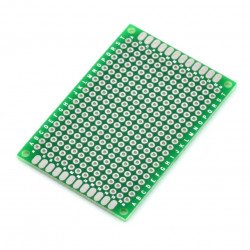
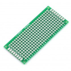
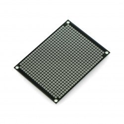
Universal double sided board 40x60mm
The board allows you to implement any electronic circuit. The holes have a raster of 2.54 mm, overall dimensions: 40 x 60 mm.
Index: PLY-02744
Index: PLY-02744
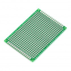
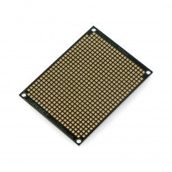
Universal double sided board 50x70mm
The board allows you to implement any electronic circuit. The holes have a raster of 2.54 mm, overall dimensions: 50 x 70 mm.
Index: PLY-02745
Index: PLY-02745
Universal double sided board 30x70mm
The board allows you to implement any electronic circuit. The holes have a raster of 2.54 mm, overall dimensions: 30 x 70 mm.
Index: PLY-02715
Index: PLY-02715
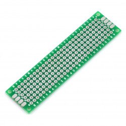
Universal double sided 20x80mm board
The board allows you to implement any electronic circuit. The holes have a raster of 2.54 mm, overall dimensions: 20 x 80 mm.
Index: PLY-02716
Index: PLY-02716
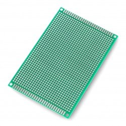
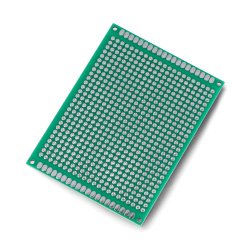
Universal double sided board 80x120mm
This double-sided, universal PCB allows you to create any electronic circuit by soldering individual components into the ready-made holes on the board. It has 1260 holes...
Index: DNG-20270
Index: DNG-20270
Universal double sided board 60x80mm
The board allows assembling of any electronic circuit by soldering the components into the ready made holes on the board. Double-sided universal board with 5 94 holes...
Index: DNG-20272
Index: DNG-20272
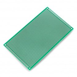
Universal double sided board 70x90mm
This universal printed circuit board (PCB) allows you to assemble any electronic circuit by soldering individual components into the ready made holes on the board placed on both...
Index: DNG-20271
Index: DNG-20271
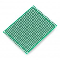
Universal double sided board 90x150mm
Double-sided universal board allows you to assemble any electronic circuit. It has 1782 holes (33 x 54) for mounting THT elements and 60 fields (2 x 30) for mounting SMD...
Index: DNG-20269
Index: DNG-20269
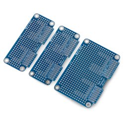
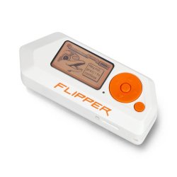
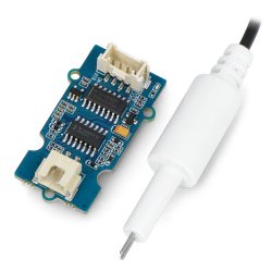
Prototype boards for Flipper Zero 3pcs.
Prototype boards for Flipper Zero that have been specially designed for direct connection to GPIO connectors. They allow you to control them without the need for...
Index: LAB-24100
Index: LAB-24100
ProtoBoard - prototyping board 572-poles - single sided - DFRobot FIT0099
Single-sided prototype plate with dimensions of 78 x 58 mm. It is equipped with 572 fields - 22 x 26, with a 2.54 mm grid and 4 mounting holes of 3 mm diameter. Ideal for quick...
Index: DFR-15088
Index: DFR-15088
ProtoBoard - prototyping board 572-poles - double sided - DFRobot FIT0203
Double-sided prototype plate with dimensions of 78 x 58 mm. It is equipped with 572 fields - 22 x 26, the raster is 2.54 mm, it also has 4 mounting holes of 3 mm diameter. It...
Index: DFR-15089
Index: DFR-15089
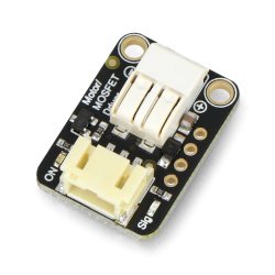
Universal board small 210 holes - MSX
A universal board with a connection layout in accordance with the contact plate. The module allows to transfer and solder the prototype system from the contact plate while...
Index: MSX-06120
Index: MSX-06120
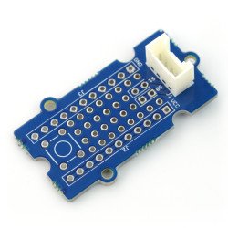
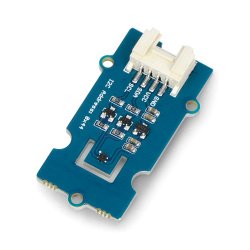
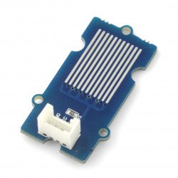
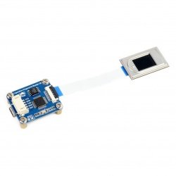
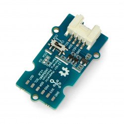
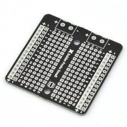
Grove - ProtoShield - prototype board
Prototype board Grove with a soldered socket. It allows for an easy access to four lines of a standard Grove-S0, S1, VCC and GND series connection cable. The layout of the...
Index: SEE-11344
Index: SEE-11344
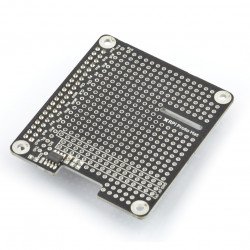
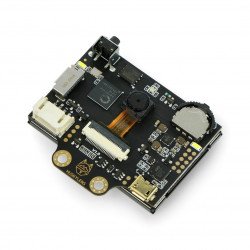
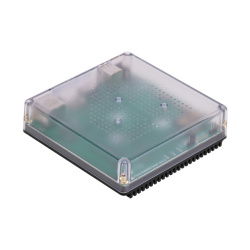
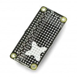
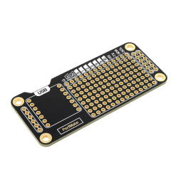
MSX Proto Hat for Raspberry Pi 4B/3B+/3B/2B
Board allows for self-creation of electronic circuits. It is connected directly to the GPIO pins of the Raspberry Pi minicomputer, version 4B / 3B+ / 3B / 2B.
Index: MSX-04552
Index: MSX-04552
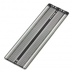
Universal board large 840 holes - MSX
A universal board with a connection layout in line with the popular 830 field contact board. The module allows the transfer and soldering of the prototype system from the...
Index: MSX-06118
Index: MSX-06118
Universal board medium 420 holes - MSX
A universal tile with a connection layout in line with the popular 400 field contact tile. The module allows the transfer and soldering of the prototype system from the contact...
Index: MSX-06119
Index: MSX-06119
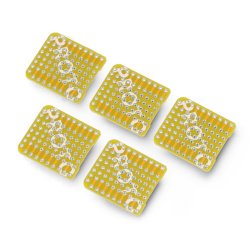
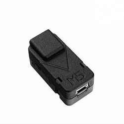
Proto Kit - CapsuleProto prototype board for M5Capsule - 62 holes - 5pcs. - M5Stack A141
The Proto Kit is a set of five perforated prototype boards specifically designed for the M5Capsule . The 26 x 24 mm board provides adequate space for soldering, placing...
Index: MSS-24376
Index: MSS-24376
Proto Board for Raspberry Pi Zero
Board allows independent creation of electronic circuits. Connected directly to the GPIO pins of the Raspberry Pi minicomputer in a version Zero.
Index: MSX-05794
Index: MSX-05794

ProtoMate universal breadboard for Raspberry Pi Zero - PiHut 106568
ProtoMate allows you to transfer prototype designs from a breadboard to a permanent, solderable pHAT design . The board features a solder pad area where pads are connected...
Index: PIH-27277
Index: PIH-27277
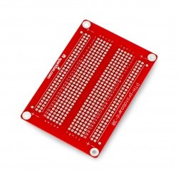
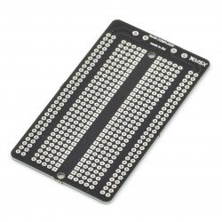
Universal board small 420 holes - SparkFun PRT-12070
Universal board with layout compatible with the popular 420 holes breadboard. The module enables the transfer and soldering of the prototype system from the breadboard, while...
Index: SPF-02209
Index: SPF-02209
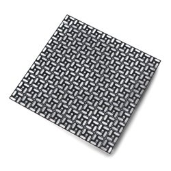
Mounting grid for PCBs - 10x10 - 2,54mm raster - Adafruit 5781
The PCB mounting grid is a proposition from Adafruit that is an alternative to standard prototype boards, which allows you to quickly connect peripheral devices and development...
Index: ADA-23824
Index: ADA-23824
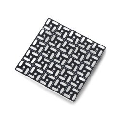
Mounting grid for PCBs - 5x5 - 2,54mm raster - Adafruit 5779
The PCB mounting grid is a proposition from Adafruit that is an alternative to standard prototype boards, which allows you to quickly connect peripheral devices and development...
Index: ADA-23823
Index: ADA-23823
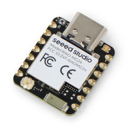
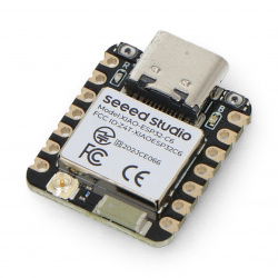
PerfMate universal printed circuit board for XIAO and QT Py - PiHut 106567
PerfMate is a perfboard- style prototyping board designed for Seeed XIAO and Adafruit QT Py modules (modules not included) . It allows you to easily transform a...
Index: PIH-27694
Index: PIH-27694

ProtoMate universal breadboard for Raspberry Pi 3B/4B/5/Zero 2 - PiHut 106569
ProtoMate is an innovative prototyping board in a HAT format , designed for users who want to transition their designs from breadboard to a permanent, solderable design. The...
Index: PIH-27279
Index: PIH-27279
Electronic printed circuit board - What can prototype boards be used for?
Electronic board - The most common soldering pad spacing used on universal boards is 100 mils , which corresponds to exactly 2.54 mm . This is the spacing between the centers of the mounting holes that most often have electronic components in through-hole housings (THT) - resistors, capacitors, goldpin connectors, integrated circuits in SIP and DIP housings, many displays, transistors, LEDs, etc. The soldering fields on the universal board are large, so no soldering, regardless of the technique used, should not pose any problems even for electronics beginners.
Some boards are equipped with SMD fields with rasters corresponding to the most popular housings of surface-mount components. In this category you will also find PCB boards dedicated to building Raspberry Pi Hat type shields. A unique, round PA07 prototype board was created for unique projects! PCB production, thanks to stable production parameters, will be characterized by repeatability, precision and high quality.
Construction of a universal printed circuit board
Two types of paths are most often used, corresponding to the arrangement of the plates in the breadboards: short paths , covering several soldering pads, and long ones , running along the edge of the board, containing several to several dozen soldering pads. The first, shorter ones, are used to make connections (nodes) between individual pins of electronic system elements.
We encourage you to check out the entire prototype boards section, where you can find, among others: SMD-DIP adapters, breadboard accessories , breadboards and many others.
Printed circuit boards - additional information
Longer paths are perfect for use as power rails - ground and supply voltage. In the case of larger universal boards, several rails are available - they can be connected to each other to increase the number of pins in a given network (e.g. ground) or used separately for several different supply voltages (e.g. symmetrical +/-5V for analog circuits). Assembling electronic components on a PCB is the fastest way, for example, to design electronic devices. Universal plates are covered with a layer of copper. Additionally, the presence of insulating material eliminates the risk of short circuit. In addition, printed circuits are susceptible to mechanical processing.
What can and cannot be built on a printed circuit board?
Simply put, printed circuit boards are suitable for soldering all typical electronic systems operating at low voltages and low frequencies.
Please remember that due to the relatively small spacing between the traces, universal PCBs are not suitable for working with voltages of several dozen or more volts, while the width of the traces limits the ability to carry higher currents. The production process includes chemical treatment.
In addition, the PCB is covered with a layer of copper. If you have additional questions about PCBs, please contact us by e-mail, via the contact form or by phone.
Universal tiles - FAQ
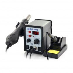
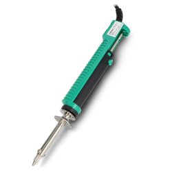
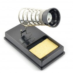
We recommend choosing Hot Air soldering irons and soldering stations . With their help, we will create truly lasting connections. They will also solve the problems of traditional soldering irons, such as the difficulty of attaching small elements - resistors or transistors . At the beginning of your workshop journey, it is also worth purchasing: a cheap board for learning SMD soldering.
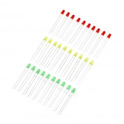
<label class="tab1Azcx1X3label" itemprop="name" for="chck2">How to choose a PCB for a set of LEDs?</label>
First, make a clear design. The life of each of them begins with a prototype, and choosing a prototype board with holes for through-hole elements is an idea to reduce costs and speed up the implementation time. We thought about it - the Adafruit LED prototype board is waiting for you in Botland in a multi-pack of 10 pieces.
PCB is a printed circuit board - the abbreviation comes from the English Printed Circuit Board . What does it mean? Laminated sandwich structure consisting of conductive and insulating layers. I'm sure each of you has seen such a perforated piece of fabric somewhere. PCBs are covered with a layer of copper and trace patterns are applied.
PCB cleaning is important. They should be washed because flux residues, dust or greasy fingerprints settle on the surface. These contaminants usually become the source of problems such as corrosion, short circuits or the inability to apply a protective coating.
The PCB can be cleaned dry or wet. The most popular cleaning methods are the use of sand, soda, dry ice, solidified carbon dioxide, ultrasound and commercially available cleaning agents. Ultrasonic cleaners are the best way to clean PCBs, which you will find in the Botland store.